ASIC Packaging
ASIC packaging technology plays a significant role in meeting performance and project objectives of production parts. Packaging format influences, size, cost, electrical performance, mechanical performance, and assembly requirements.
System To ASIC Offers World-Class Packaging Solutions
System To ASIC uses world-class packaging facilities all over the world to assure high quality redundant assembly capability. These facilities provide rigorous package reliability qualification such as AEC-Q100, and maintain stringent quality standards such as IATF 16949, allowing delivery into very demanding markets. From state of the art chip scale package profiles, to plastic leadless (QFN, SLP, MLF), to die in waffle pack, STA provides packaging solutions that meet your budget, performance, and size objectives.
The Right Package Technology for Your Application
STA delivers ASIC solutions into a wide range of applications. We understand the role packaging technology plays in achieving production efficiencies and in-field success. As part of our ASIC design services, we apply our experience and in-depth awareness of your application to ensure an optimal package format(s) is part of your ASIC solution.
Numerous Package Styles To Choose From
Over the years, a daunting number of package styles have been developed to solve various issues including, technology advancements, pin count, size, thermal performance, automated production, cost, etc. Wikipedia offers an informative overview describing many of the available ASIC packaging forms. STA can package your part in many of these forms to meet a range of project demands from legacy to modern.
Leadless: A Go-To Packaging Format for Many Mixed Signal ASIC Applications
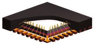
Cross Section of Leadless Package
Among the sea of packaging options offered, there is a format that meets the demands of many mixed signal ASIC applications; a plastic, leadless package that is very near chip scale. Several industry names describe the leadless package style, including, QFN (Quad Flat No-lead), SLP (Small Leadless Package), and MLF (Micro Lead-frame). There are also variants of these packages addressing, RF performance, reduced height, thermal performance, and lowering cost for high volume production. While the list of options is still long, they are more similar than different, offering good electrical and thermal performance, low cost, and multi-vendor sourcing.
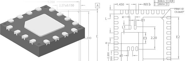
Bottom View of Leadless Package Showing Exposed Pad
Leadless Package Technology Is a Good Option
Leadless plastic packaging has become the go-to format for a lot of STA projects. While the technology is not a one size fits all solution, it is currently one of the best options for a majority of mixed signal ASIC designs.
QFN , SLP, MLF Attributes:
- Small Footprint – Near Chip Scale
- Excellent Thermal Management – Exposed Pad to PCB
- Good RF Performance
- Ease of PCB Assembly
- Low PCB Construction Demands
- Low Cost for Low & High Volume
- High Availability – Many Manufacturers
WLCSP: The Ultimate In Small Size & Signal Integrity
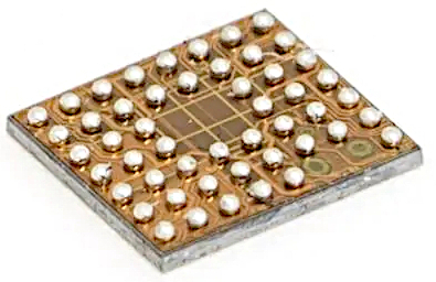
Bottom View of WLCSP with Bump on RDL
Wafer Level Chip Scale Package technology offers excellent performance, low cost, and the absolute smallest footprint available for single die packaging. With WLCSP, the package literally is the size of the die. Another feature of WLCSP is very high signal integrity for applications susceptible to parasitic inductance and capacitance. This is due to extremely small pads and ultra short path length from IC pad to PCB. Additionally, WLCSP is one of the lowest cost packaging forms available for high volume applications
A High Performance Package for High Volume
WLCSP is high a performance low cost ASIC package technology that continues to gain wide spread use, particularly in high volume mobile and consumer applications. However, this package does require advanced PCB fabrication technology and assembly facilities, which for now, limits use of main stream PCB and assembly vendors. As more vendors advance their capabilities, this package will see use in a broader range of applications.
WLCSP Attributes:
- Smallest Footprint – Chip Scale
- Good Thermal Management
- Excellent RF Performance
- High reliability interconnect and shock resistance
- Lowest per Part Cost at High Volume
- Specialized PCB Assembly Required
- Demanding PCB Geometry and Surface Finish
- High Availability – Many Manufacturers
System To ASIC Will Help You Choose the Right Package Technology
System To ASIC delivers turn-key ASIC solutions tailored to your project goals. We explore your application in-depth so we can leverage our expertise to guide you through successful ASIC development. System To ASIC provides a broad range of package options and will help you select the right package technology for your application. Contact us today to learn more.
ASIC Packaging Options
ASIC Packaging – Popular Drawings
Package Specifications
Below are links to our most popular packages:
Special Order
Ceramic packages, open cavity, flip-chip and multi-chip modules available on request. Contact System To ASIC for more information.